What do you do?
We all know the that different materials we interact with every day have different properties. A material's mechanical properties are whether it is hard or soft and how easy it is to break or bend. Electrical properties refer to material's ability to conduct electricity, like highly conductive copper in a wire or nonconductive wood. Thermal properties describe how easy a material is to heat up, like a frying pan which heats up quickly or oven mitts which heat through very slowly. We take advantage of the properties of the materials around us in everyday activities like the way we cook food to how we build machinery and electronics. All of the properties we utilize daily occur in three dimensional materials, but ten years ago a new class of materials with unique and sometimes counterintuitive properties was discovered: two dimensional materials. Over the past ten years the imaginations of scientists and engineers have been captivated by these new 2D materials as we discover their fascinating characteristics and envision their potential applications, particularly in electronics. In fact, 2D materials are already being used by some companies to make more efficient touchscreens and solar panels. [1] [2] However, more investigation into 2D materials must be done before they can be as widely applied and useful as they are predicted to someday be. In our lab we work to gain new insights into the structure and properties of 2D materials.
What exactly is a 2D material?
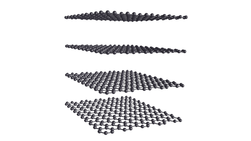
To explain what a 2D material is, we’re going to use as an example the first 2D material ever isolated by scientists. This material is called graphene, and it’s a 2D form of graphite. When you look at the core of a pencil, you see a big cylindrical hunk of graphite. In physics terms, we would refer to this as bulk graphite. On an atomic level, this graphite is made of many stacked sheets of carbon atoms arranged in a honeycomb pattern, modeled in the picture below.
[3]
Graphene, the 2D form of graphite, is a single sheet of carbon atoms. Any 2D material is just a single or a couple atomic sheets of the bulk material, but only certain materials are stable in a single atomic layer, so only certain materials have a 2D counterpart. Each atom sheet is about 0.1 nm, or 0.0000000001 meters, thick. To give you an idea of how small these layers are, let’s say you just sharpened your pencil and the graphite tip is now 3 mm long. In the sharpened tip of your pencil, there are about 30,000,000 atom sheets! On a scale that we can more easily visualize, if the thickness of your average piece of printer paper is the height of the Empire State Building, the thickness of a two dimensional material would be the height of a beetle standing next to it.
Graphene, the 2D form of graphite, is a single sheet of carbon atoms. Any 2D material is just a single or a couple atomic sheets of the bulk material, but only certain materials are stable in a single atomic layer, so only certain materials have a 2D counterpart. Each atom sheet is about 0.1 nm, or 0.0000000001 meters, thick. To give you an idea of how small these layers are, let’s say you just sharpened your pencil and the graphite tip is now 3 mm long. In the sharpened tip of your pencil, there are about 30,000,000 atom sheets! On a scale that we can more easily visualize, if the thickness of your average piece of printer paper is the height of the Empire State Building, the thickness of a two dimensional material would be the height of a beetle standing next to it.
How do you make 2D materials?
It’s hard to even fathom such thin materials, so is it hard to make them? Producing small amounts of 2D material actually isn’t very hard at all – in fact, you probably make small amounts of graphene every time you write with a pencil. Making graphene like this is not very different from the first way graphene was produced in a lab, and would be considered mechanical exfoliation. Exfoliation refers to removing very thin layers of material from the bulk, and mechanical describes the fact that mechanical force (you putting your pencil on the paper) is used to power the exfoliation. The first graphene was produced in a lab by a mechanical exfoliation technique using scotch tape to remove very thin layers from a bulk piece of graphite. The graphite on the scotch tape was then pressed onto a substrate. [5] A substrate is another piece of material that acts as a base to which the graphite and graphene adhere. In our lab, we use this method to make 2D materials along with another mechanical exfoliation technique in which we use razors to shave thick layers of material on a substrate down to 2D thickness. Additionally, some of our samples are made by collaborating laboratories.
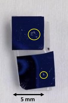
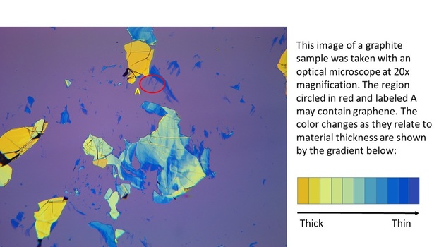
Pictured below on the left is a mechanically exfoliated sample made in our lab. Circled in yellow are chunks of the exfoliated material, in this case graphite. To the right is an image of a similar sample taken under an optical microscope at 20x magnification. The color gradient to the right of this image shows how we can tell the approximate thickness of the exfoliated material by the color it appears. In the optical microscope image, a region that probably contains graphene is circled in red and labeled "A".
Pictured below on the left is a mechanically exfoliated sample made in our lab. Circled in yellow are chunks of the exfoliated material, in this case graphite. To the right is an image of a similar sample taken under an optical microscope at 20x magnification. The color gradient to the right of this image shows how we can tell the approximate thickness of the exfoliated material by the color it appears. In the optical microscope image, a region that probably contains graphene is circled in red and labeled "A".
|
|
How do you learn about 2D materials?
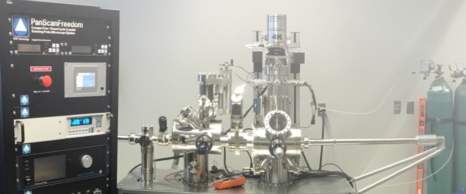
The properties of a material arise from its atomic structure, so an important step in learning about a material is to image it on the atomic level. This is done using a scanning tunneling microscope (STM). Below is a picture of our STM.
Scanning tunneling microscopes (STM) produce images of the atoms that make up a material so we can see the pattern in which atoms in a material are bound. Materials are imaged by an STM by probing them using a tip so sharp that the end composed of a single atom. The tip is brought extremely close to the material, about 1 nanometer away. At this range, a voltage is applied and a phenomenon called quantum tunneling causes electrons to tunnel, or jump, from an atom in the material to the atom on the end of the tip. This movement of electrons creates a current. The strength of the current changes depending on the distance between the tip and the atom it is interacting with in the material. When the tip is closer to the atom, the current is higher, and when the tip is farther from the atom, the current is lower. Atoms are approximately spherical, so we can think of the surface of the material as a collection of spheres arranged in some pattern. During imaging, the tip can be moved across the surface at a constant height above the surface. When the tip is directly over an atom, it is closer to the surface (left side of the image below) than when it is between two atoms (right side of the image below).
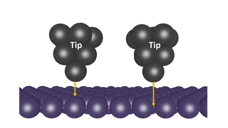
Since the current between the tip and the material changes depending on the distance between the tip and the material, we can determine how far the tip is from the surface by measuring the current. Higher currents indicate that the tip is closer to the material, meaning that there is an atom right below it. Lower currents indicate that the tip is farther from the material, meaning that it is between atoms. [4]
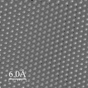
So how does this make an image? An image is made by a computer that receives the current measurements and produces a corresponding pixel. For higher current measurements, the computer produces lighter pixels, and for lower current measurements it produces darker pixels. Eventually, this produces a black and white image that shows atoms in white and the space between them in black, and shows their approximate round shape by a gray scale between. A black and white STM image taken at our lab is shown below.
So how does this make an image? An image is made by a computer that receives the current measurements and produces a corresponding pixel. For higher current measurements, the computer produces lighter pixels, and for lower current measurements it produces darker pixels. Eventually, this produces a black and white image that shows atoms in white and the space between them in black, and shows their approximate round shape by a gray scale between. A black and white STM image taken at our lab is shown below.
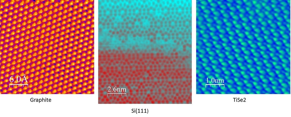
STM images are often colored to highlight areas of interest on the material. It also makes them really pretty and cool to look at. A few colored STM images taken at our lab are shown below. The first image is the colored version of the black and white image above.
In addition to imaging materials, we take electrical measurements across the materials to learn about their electrical properties, such as electron mobility. Electron mobility is the tendency of electrons in a material to move around. A material with high electron mobility will have electrons that move around very easily, and a material with low electron mobility will have electrons that don’t tend to move a lot at all. Materials with high electron mobility tend to also have high conductivity, making them good for applications in electronics, like the phone or solar panels mentioned earlier.
Cool! Can I get involved?
We love helping people learn about science! If you're intrigued by what we do and want to know more, or if you have some questions we didn't answer here, please contact us, send us an email, or even tweet @UNH2D. If you're in the area and want to learn more and see our facilities in person, we'd be happy to arrange a lab tour.
Bibliography
[1] Tsai, Meng-Lin, and Al Et. Monolayer MoS2 Heterojunction Solar Cells. ACS Nano 8.8 (2014): 8317-322. 1 June 2016.
[2] Wan, Adrian. “Graphene-based Chinese smartphone technology could 'boost battery life by 50 per cent'.” South China Morning Post. 5 March 2015. 1 June 2016.
[3] Graphene Nanoplatelets Products. Cheap Tubes. N.p., n.d. Web. 01 June 2016.
[4] "Scanning Tunneling Microscopy." University of Utah. Web.
[5] Novoselov, K. S., Geim, A. K., et al. (2004). Electric field effect in atomically thin carbon films. Science, 306(5696), 666-669.
